The idea occurred to Jack Kilby at the height of summer, when everyone else was on vacation and he had the lab to himself. It was an idea, as events would prove, of literally cosmic dimensions, an idea that would eventually be honored in the textbooks with a name of its own: The Monolithic Idea. But at the time–it was July, 1958–Kilby only hoped that his boss would let him build a model to see if the idea could work.
The Monolithic Idea occurred (independently) to Bob Noyce about six months later. Noyce, a more businesslike sort than Kilby, recognized right away that the concept of integrating all the parts of an electronic circuit–resistors, transistors, capacitors, diodes–in a single (“monolithic”) block of semiconductor material was a major technological and commercial breakthrough.
Noyce’s instinct, as usual, was correct. In the quarter-century since these two Americans got their bright idea, the monolithic integrated circuit–better known as the semiconductor chip–has changed the daily life of the world. The chip is the heart of deep-space probes and deep-sea sensors, of toasters, typewriters, and data transmission networks, of pacemakers and Pac-Man, of clocks, computers, cameras, and the Columbia space shuttle. It has made possible astounding reductions in the size, cost, and power requirements of electronic equipment. The computers of the 1950’s, gargantuan collections of tubes and wiring that filled a large room and consumed the power of a locomotive, would be easily outdistanced by a modern $200 microcomputer that fits in your pocket and is powered by penlight batteries.
As a technological matter, the integrated circuit seems almost too good to be true. It is smaller, lighter, faster, cheaper to make, cheaper to use, and more reliable than the traditional electronic circuits, wired together from individual parts, that it replaced. Its raw material, silicon, is derived from ordinary sand and is one of the planet’s most plentiful elements. The manufacture of microchips can be a demanding, tedious task, but it is essentially a non-polluting activity.
The social implications are as yet unclear. The National Academy of Sciences calls the new wave of microelectronics “the Second Industrial Revolution”, and suggests that its effect on society may be greater than the first. Studies of the impact of this revolution will no doubt keep legions of sociologists and psychologists gainfully employed for decades to come.
One key social influence that is apparent, though, is that the integrated circuit has decentralized computer capability–and thus averted a problem that caused much concern a generation ago. When the first computers were developed, writers painted a grim picture of a “1984” society in which ordinary people would be at the mercy of the few giant entities that could afford and understand these awesome machines. Today, thanks to the Kilby/ Noyce invention, ordinary people are buying computers by the millions and junior-high students routinely use them for schoolwork or play. By 1984, according to industry estimates, about 35 million Americans will have computers of their own at home.
There was a time when the people who improved the daily lot of mankind with a bright idea held considerable prominence. Men like Edison, Bell, and Ford were heroic figures in their day, household names around the globe. Now, in a world where individual achievement is so often dwarfed by huge corporate and governmental enterprises, innovators toil in relative anonymity. Although Jack Kilby and Bob Noyce have won numerous awards and widespread recognition within the electronics community, they are unknown to the world at large. Many–possibly most–Americans have heard of the “miracle chip”; hardly any could name the men who made the miracle.
Latter-Day Edisons
Perhaps, then, it is time to meet these two latter-day Edisons.
Jack St.Clair Kilby and Robert N. Noyce are both products of the heartland–Noyce was the son of a Congregationalist minister in Grinnell, Iowa; Kilby’s father ran the local power company in Great Bend, Kansas. Both decided early on to make a career in electronics. Both were in their thirties when they focused on the need for integrated circuits, and both came up with the same basic solution at about the same time. For all that, though, if you spend some time with each man, the most striking thing about them is what different people they are.
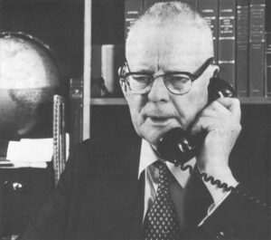
Noyce, a wiry, athletic-looking man who wears fashionable clothes and silver-rimmed aviator glasses, seems considerably younger than his 54 years. He is a quick, outgoing fellow who conveys the intense self-assurance of a jet pilot (he does, in fact, fly his own small plane). He has been successful at just about everything he has ever tried; after earning his Ph.D. in physics at MIT in 1953, he was offered jobs by every major electronics firm, and was eventually invited to join the elite group of pioneers working with William Shockley, the co-inventor of the transistor who was then the most important man in the field.
Noyce likes to work in groups, and needs companions to help him work out his ideas. In addition to his technical achievements, he has founded two of the most successful semiconductor firms and parlayed his stock holdings into a net worth that colleagues estimate at $100 million.
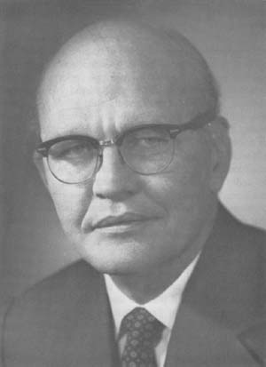
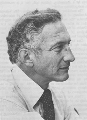
Kilby, a lanky 59-year-old with a round, leathery face and just a few wayward tufts of gray hair remaining on his balding head, is a quiet, gentle, grandfatherly type. With his utterly unassuming manner and slow, soft way of talking, he seems somewhat out of place in his high-tech world; you’d rather expect to meet a man like this rocking peacefully on the porch of some country store.
Professionally, Kilby was something of a late bloomer. He flunked the entrance exam at MIT, and after he earned his Electrical Engineering degree at the University of Illinois in 1947, he went to work for a Milwaukee firm called Centralab–because it was the only place that offered him a job. He was there more than ten years before moving on to a better position at Texas Instruments.
Though he is an extremely friendly person, Kilby does his best work alone. Since 1970, when he took a leave from Texas Instruments, he has been working in a small Dallas office on his own. He lists his occupation as “self-employed inventor”–a calling that has brought him much freedom and satisfaction, he says, but “marginal” economic rewards.
Unmatched Pair
Still, this unmatched pair does have one striking attribute in common: a talent for, and a genuine delight in, thinking through problems. Not surprisingly, considering what they have achieved, both Noyce and Kilby have enormous faith in the power of the human mind. To them, a problem–be it a minute flaw in a micro-miniature circuit or some pervasive dilemma of social policy–exists to be solved, and with the right preparation a solution can be found.
Both inventors, characteristically, have given considerable thought to the mental process involved in invention. Greatly simplified, the process both describe is a two-stage affair that moves from saturation to concentration. At first, the problem-solver has to soak up every fact he can, no matter how remotely related, about the problem: “You accumulate all this trivia,” Kilby says, “and you hope that sometime maybe a millionth of it will be useful.” Thereafter, the inventor has to concentrate intently on the issue at hand. If you ask these men where they do their most productive thinking, neither has an answer. They can work anywhere–in the office, at home, in a grocery store check-out line–where they have a moment to tune out everything else and think deeply about the problem.
The final and essentially indescribable element in the inventive process is the imaginative leap–the creative break with past ways of doing things. “You can sort of get stuck in a rut when you’re working on something,” Noyce says. “And what you have to do is fire up your imagination…you have to jump to the new idea.”
The entire field of semiconductor electronics was a new idea in the 1940’s, when Noyce and Kilby were in college. The physical principles of electronic charges moving in semiconductor materials like germanium and silicon were as yet vaguely understood, and professors were struggling, not always successfully, to find ways to teach this unfamiliar subject. The one thing Kilby remembers from his undergraduate electronics lab is that none of the experiments turned out the way the professor said they would.
Things began to fall more clearly into place in 1947, when William Shockley’s research team at Bell Labs achieved a major breakthrough that was seminal to the microelectronics revolution: the invention of the transistor.
Before The Transistor
Until the transistor came along, electronic equipment had been based on a cumbersome device known as the vacuum tube, or radio tube. The tube was, basically, the same thing as an electric light bulb; in a vacuum sealed by a glass bulb, current flowed through a wire filament, heating the wire and giving off light. Early in this century scientists found that if you ran some extra wires into the bulb, it could perform two key electronic functions. First, if connected to an antenna, it could pull a weak radio signal out of the air and strengthen, or “amplify”, it enough to convert the signal to sound. This made radio, and later television, possible. Second, a properly wired tube could switch readily from “on” to “off”. This capability was essential for digital computers, in which logical decisions and mathematical computations are made by various combinations of “on” and “off” signals.
But vacuum tubes were big, expensive, fragile, and power-hungry. If a number of tubes was grouped together, as in a computer, all those glowing filaments gave off heat in great quantities. The transistor eliminated all these drawbacks in one fell swoop. The transistor had no glass bulb, vacuum, or hot filament. It was a “solid state” device, in which amplification and rapid switching were achieved by the movement of charges through a solid block of semiconductor material.
The advent of the transistor provided a major impetus for expanded research in semiconductor physics, and that work, in turn, led to steady improvements in transistors. By the early 1950’s, “solid state” was replacing vacuum tubes in radios, hearing aids, and other electronic gear. The burgeoning computer industry made a strong market for transistors, as did the military, which needed small, reliable parts for ballistic missiles and the nascent space program.
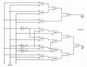
But the transistor, too, had a serious disadvantage. For most applications, large numbers of transistors–thousands of them in computers–had to be wired into circuits with equally large numbers of traditional components like resistors and capacitors. It was mostly hand work, creating obvious problems of time, cost, and reliability. There was another, less obvious difficulty as well. The more wiring there is in a circuit, the farther electric charges have to travel to make it work. Since charges travel about a billion feet per second, this was no great problem in most equipment. But in computers, where charges must switch to and fro millions of times to carry out even simple programs, the size of transistorized circuits created serious problems. The complexity of transistor circuits–a problem the engineers called “the tyranny of numbers”–was a tall hurdle blocking further progress in microelectronics.
Engineers around the world hunted a solution. The U.S. Air Force placed a multi-million-dollar bet on a concept called “molecular electronics” that never left the starting gate. The Army and Navy, true to form, spurned the Air Force approach and pursued theories of their own. Private firms, including Texas Instruments, mounted large-scale research efforts. Texas Instruments recruited engineers from coast to coast for the task, and one of the men it hired was a lanky 34-year-old engineer from Milwaukee named Jack Kilby.
When Kilby arrived in Dallas in May of 1958, one of the hot ideas at Texas Instruments was a circuit design called the “micromodule”, in which all the parts of a circuit were to be manufactured in the same size and shape. The parts could then be snapped together like a wood block puzzle, obviating individual wiring connections. “From the beginning, I didn’t much like it,” Kilby recalls. For one thing, it didn’t solve the basic problem of numbers; for another, Kilby had a sense that it just couldn’t work. But the brand-new employee was in no position to tell his bosses that their grand idea was no good.
Texas Instruments had a mass vacation policy then, and everyone took off the same two weeks in July. The new employee had not yet earned vacation time, so Kilby was left alone in the lab. If he was ever going to find an alternative to the micromodule, here was the chance. He started off on the first phase of problem-solving, saturating himself with every conceivably relevant fact about his new firm and the problem it wanted him to solve.
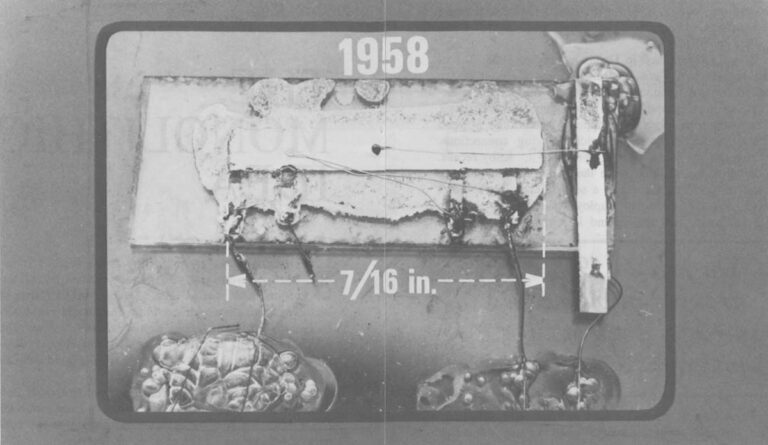
Kilby learned that Texas Instruments had spent millions developing machinery and techniques for working with silicon. “If T.I. was going to do something,” he explains, “it probably had to involve silicon.” What could you do with silicon? Shockley’s invention had proven that a block of silicon could replace the vacuum tube. Silicon was also commonly used in diodes. It dawned on Kilby that he could make a capacitor out of silicon; it would not perform as well as the standard metal and ceramic capacitor, but it would work. For that matter, you could make a silicon resistor, too–not as good as the standard carbon resistor, but it would work And if all these circuit components could be made from the same material, why not fabricate them all in a monolithic block of that material? You wouldn’t have to wire the parts together, and the electric charges would need to travel only minute distances. On July 24, 1958, Kilby scratched in his notebook a rough sketch of an integrated circuit.
Kilby’s bosses returned from vacation, eager to get cracking on the micromodule. Kilby showed them his notebook; with a little prodding, they agreed to make a model of this strange circuit on a chip. The project was not a high priority, and two months passed before a group of engineers gathered in Kilby’s lab to watch him hook up a battery to the world’s first integrated circuit. The idea worked perfectly. A new era in electronics had begun.
At this time Robert Noyce and several colleagues were busily involved in transistor development at the Santa Clara, CA, firm they had recently founded, Fairchild Semiconductor. A major problem in building transistors then was making precise, reliable connections between the different segments of the transistor. It was hard to construct metal connections on the semiconductor material that made contact with a single precise spot on the transistor. Early in 1958 a Fairchild physicist, Jean Hoerni, had worked out a new method of making connections–the “Planar” process, in which a flat planar layer of insulating material was spread atop the semiconductor like icing on a cake. Connections could be poked through this “icing” to the exact point of contact.
Like many others, the 31-year-old Noyce had been thinking about the complexity of transistor circuits and the clear need to deal with “the tyranny of numbers.” His initial ideas, involving adaptations of traditional circuit techniques, didn’t work. The planar process, though, “was something that got me out of the rut,” he recalls. Not suddenly, but gradually, during the winter of 1958-59, he developed a new idea. If separate sections of a transistor could be connected within a single block of silicon, maybe you could put other circuit elements in the same block, coat the whole thing with the planar…icing”, and connect all the parts within a monolithic circuit. Noyce talked things over with his colleagues, discarding some ideas, refining others. These inchoate thoughts all came together on Jan. 23, 1959, and he wrote in his notebook a rough proposal for making “multiple devices on a single piece of silicon in order to make interconnections between devices as part of the manufacturing process, and thus reduce size, weight, etc. as well as cost….”
Twenty-four years later, the two inventors can still recall the birth of the integrated circuit with considerable clarity, even though both men have moved on to new endeavors. A few years after the invention, Noyce co-founded a brand new firm, Intel (for “Integrated Electronics”), which has become a giant of the industry. In the process, Noyce says, he “gradually drifted” from engineering to management. Today he is vice-chairman of Intel in Santa Clara. A gregarious person and an impressive speaker, he has become a senior statesman and leading spokesman for the semiconductor industry. As one electronics executive puts it, Noyce is “the Mayor of Silicon Valley.”
Kilby, the quiet introvert, is still happily and creatively engaged in inventing. He has more than 50 patents to his credit, including the first patent for the pocket calculator, one of the most successful new consumer products in industrial history. Since he went to work on his own a dozen years ago, the scope of his work has expanded. At his wife’s suggestion, he invented a device that screens telephone calls so your phone won’t ring unless the call is one you want to take. For the past few years he has focused on a household solar energy generator.
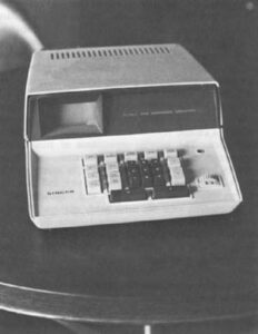
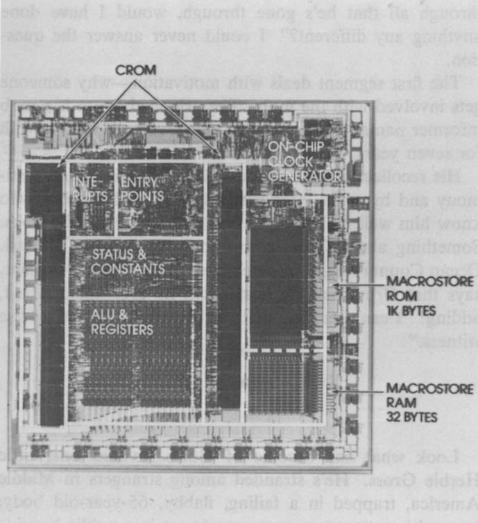
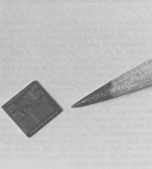
Both men are modest about their great idea, but neither can completely conceal the parental pride they feel in the progress of their brainchild. The first integrated circuits on the market contained about a dozen circuit components and cost $450; today a chip several hundred times more complex costs one/one-hundredth as much. As engineers have learned to cram more and more circuitry onto a chip, the integrated circuit has reached levels of complexity that even the inventors find amazing. Many models today incorporate more than 100,000 components, all on a sliver of silicon about the size of the word “CHIP” on this page. There are circuits that put an entire computer on a single tiny chip; these “microprocessors” are at work today in hundreds of products from cars to color TVs to the latest model Cuisinart.
And the end is not in sight. Noyce got thinking a while back about the fundamental physical limits of microelectronics. He concluded that integrated circuits, and the computers built from them, could be made hundreds of times more complex than those available today. Characteristically, that got Noyce thinking about another question. “The next question is, Who can use that intelligence?” Noyce says. “What will you use it for? That’s a question technology can’t answer.”
©1982 T.R. Reid
T.R. Reid, a reporter on leave from the Washington Post, is investigating the U.S. semiconductor industry.